 القضبان
 الخرز والكرات
 البراغي والصواميل
 البوتقات
 الأقراص
 الألياف والأقمشة
 الأفلام
 فليك
فليك
 الرغاوي
 رقائق معدنية
 الحبيبات
 أقراص العسل
 الحبر
الحبر
 صفائح
صفائح
 الكتل
الكتل
 التشابك
 غشاء معدني
 اللوحة
 المساحيق
 قضيب
قضيب
 الصفائح
 البلورات المفردة
 هدف الاخرق
 الأنابيب
 الغسالة
 الأسلاك
 المحولات والآلات الحاسبة
 اكتب لنا
ثاني أكسيد القصدير النانوي: مادة متعددة الوظائف في مجال أشباه الموصلات
1 Introduction
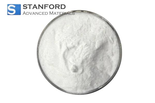
Nano-sized tin dioxide (SnO2) is a wide-bandgap semiconductor material (bandgap approximately 3.6 eV) that has become one of the core materials in the semiconductor industry due to its unique physical and chemical properties. Its conduction band comprises Sn 5s orbitals, featuring a small effective electron mass and high spatial overlap, which endows the material with high electron mobility, maintaining excellent conductivity even in the amorphous state. With particle sizes controllable down to the 10-nanometer level and a purity of 99.99% in pale-yellow powder, it plays an irreplaceable role in multiple high-tech fields.

Fig. 1 Nano Tin Oxide Powder
2 Material Structure
Nano-sized tin dioxide (SnO2) serves as a core material for modern semiconductor devices, with its exceptional performance fundamentally rooted in its unique material structure. At room temperature and pressure, SnO2 exists stably in a tetragonal rutile structure (space group: P42/mnm), with its three-dimensional framework composed of tin-oxygen octahedra forming the functional foundation of the material. The unit cell parameters (a = b = 4.737 Å, c = 3.186 Å) reveal its anisotropic compression along the c-axis—each Sn4+ ion is coordinated by six oxygen atoms in a distorted octahedral arrangement (bond length 2.05–2.06 Å). In contrast, the oxygen ions connect three tin atoms in a planar triangular configuration, forming a rigid [SnO6] octahedral chain network. This highly symmetrical crystal framework not only endows the material with excellent thermal stability but also provides an ideal pathway for electronic transport.
Table 1: Structural Features of Nano SnO2
|
Structural Parameters |
Value/Description |
Physical Significance |
|
Unit Cell Parameters |
a = b = 4.737 Å, c = 3.186 Å |
Compressed along the c-axis direction, exhibiting anisotropy. |
|
Sn-O Bond Length |
2.05 Å (equatorial plane), 2.06 Å (axial) |
Highly symmetrical octahedral coordination environment |
|
O-Sn-O Bond Angle |
79.6° (adjacent O), 130.4° (relative O) |
Determining electronic orbital overlap and band structure |
|
Coordination Number |
Sn⁴⁺: 6, O²⁻: 3 |
Forming a stable three-dimensional network framework |
At the electronic level, the wide bandgap semiconductor properties of SnO2 (3.6 eV) stem from its unique band structure: the conduction band bottom is formed by strong overlap of Sn 5s orbitals, resulting in a wide and flat band with an electron effective mass as low as 0.3m₀, yielding a mobility as high as 250 cm2/V·s; the valence band top, however, originates from localized O 2p orbitals, with a hole mobility of less than 10 cm2/V·s. This significant electron-hole asymmetry, combined with shallow donor levels formed by oxygen vacancies (0.03–0.15 eV below the conduction band bottom), naturally establishes the material's n-type conductivity.
Structural transformations occur when material dimensions enter the nanoscale range (10–50 nm). The proportion of surface atoms increases to over 30%, low-coordination tin-oxygen atoms form dangling bonds, leading to surface lattice expansion (lattice constant increases by 1–3%) and local disorder. The broadening of the 620 cm^-1 peak in Raman spectroscopy confirms this nano-induced defect proliferation—oxygen vacancy concentrations can reach 10^20 cm^-3, an increase of two orders of magnitude compared to bulk materials. Meanwhile, quantum confinement effects become evident when particle sizes are less than 5 nm, with the bandgap widening to 4.1 eV and the ultraviolet absorption edge shifting to shorter wavelengths. Morphology control further introduces dimensional effects: zero-dimensional nanoparticles (such as VK-Sn30) expose highly active crystal faces; one-dimensional nanowires enable directed electron transport along the [001] direction; and three-dimensional hierarchical structures (such as nanowires) create multi-level diffusion channels. These structural reorganizations at the nanoscale transform the material from a static crystal into a dynamic functional carrier.
Defect engineering further unlocks the depth of performance control. Oxygen vacancies (Vₒ) act as double-electron donors to dominate conductivity regulation, while tin vacancies (Vₛₙ) serve as dominant compensating carriers, and interstitial tin (Snᵢ) forms donor levels. Positron annihilation spectroscopy reveals a significant increase in Vₛₙ concentration within the nanoparticles, and the synergistic effect of these intrinsic defects constitutes a microscopic switch for electrical behavior.
3 Core Characteristics
3.1 Excellent Electrical Performance
The conductivity mechanism of SnO2 stems from its unique electronic structure: the Sn 5s orbitals form a wide and overlapping conduction band, resulting in extremely low electron migration resistance. This characteristic enables nano-SnO₂ thin films to maintain high transparency (>80%) while achieving resistivity as low as 10^-4–10^-6 Ω·cm, far exceeding that of traditional oxide semiconductors.
3.2 Unique Optical Properties
It exhibits high transmittance in the visible to near-infrared wavelength range (350–2500 nm) and strong absorption in the ultraviolet region. Its low refractive index (≈2.0) and extinction coefficient make it an ideal choice for transparent conductive electrodes (TCOs), particularly for devices requiring high transmittance, such as touchscreens and photovoltaic cells.
3.3 Outstanding Surface and Catalytic Activity
Nano-sized SnO2 has a huge specific surface area (up to 80 m2/g) and lots of active sites on its surface. When gas molecules stick to the surface, it quickly changes the resistance, which is why it's a key material for sensing gases.

Fig. 2 Controlling Nitrogen Dioxide Sensitivity by Regulating the Concentration of Defects on The Surface of Tin Dioxide
4 Key Application Scenarios in The Semiconductor Field
4.1 Gas Sensor
Nano-sized tin dioxide-based gas sensors have become a core technology in environmental monitoring, with their exceptional performance deeply rooted in the intrinsic structural properties of the material. When target gas molecules (such as CO, formaldehyde, or NOx) come into contact with the specially designed SnO2 sensor surface, gas adsorption immediately triggers a chain reaction of electron transfer, In terms of performance, this mechanism based on surface electron exchange endows the sensor with remarkable sensitivity: it can reliably detect trace contaminants at the ppm level (parts per million), with a detection limit for formaldehyde as low as 0.1 ppm. Even more impressive is its dynamic response capability, enabling the sensor to identify gases within seconds (e.g., response time for CO <5 seconds) and quickly return to baseline after the gas source is removed. This real-time capability makes toxic gas warning systems feasible in industrial settings. Its stability is equally impressive, maintaining over 90% of its initial sensitivity in an 85% high-humidity environment, overcoming the traditional sensor's susceptibility to environmental interference.
The key to this performance breakthrough lies in the precise design of the multi-level nanostructure. The three-dimensional flower-like SnO2 microspheres, synthesized via the hydrothermal method, are self-assembled from two-dimensional nanosheets, with their surfaces densely covered by secondary pores of 10–20 nm. This multi-level structure not only increases the specific surface area to 80 m2/g (approximately three times that of solid particles) but also creates interconnected gas diffusion channels. When target gas molecules enter, the unsaturated bonds at the edges of the nanosheets (such as unsaturated Sn³⁺ sites) serve as priority adsorption sites to capture molecules, while the hierarchical pore structure forms "nanoreaction cavities" that prolong gas residence time and promote deep reactions. Experimental results demonstrate that this structure enhances sensitivity to ethanol by 17 times compared to conventional nanoparticles and accelerates response speed by 40%. Reducing gas molecules donate electrons to the material, while oxidizing gases abstract electrons. This redistribution of surface charge directly modulates the material's resistance, generating a reversible signal of resistance change. It is precisely the abundant oxygen vacancies and highly active crystal faces on the SnO2 surface that provide an ideal reaction platform for the rapid cycling of gas adsorption and desorption.

Fig. 3 SnO2 SEM Image
This synergistic effect of "surface chemistry and nanostructure" makes SnO2 sensors indispensable in smart homes, industrial safety, and in-vehicle air quality monitoring. With the explosive demand for distributed sensor networks in the IoT era, miniaturized, low-power sensors based on nanoengineered SnO2 are ushering in a new era of environmental sensing, and it all starts with the active oxygen vacancies and carefully constructed nanotopology at the atomic level of the material.
4.2 Solar Cells
In the wave of technological innovation surrounding perovskite solar cells (PSCs), nano-tin dioxide is replacing traditional titanium dioxide (TiO2) in a disruptive manner and becoming the core material of the new generation of electron transport layers (ETLs). The core advantage of this revolutionary application is first reflected in its revolutionary low-temperature process adaptability - SnO2 thin film can be formed with high quality under mild conditions below 150°C, completely getting rid of the traditional TiO2's dependence on high-temperature sintering at 500°C. This feature not only greatly reduces energy consumption but also achieves perfect compatibility with flexible polymer substrates (such as PET, PEN), paving the way for foldable and lightweight photovoltaic devices.
The significant performance breakthrough stems from the precise energy level matching between SnO2 and perovskite materials. Compared to TiO2 (with a conduction band bottom of approximately -4.0 eV), the conduction band bottom of SnO2 is at -4.3 eV, forming a steeper energy level gradient with the perovskite light-absorbing layer (such as MAPbI3 with a conduction band of approximately -3.9 eV). This optimized band structure acts like an efficient "electron slide", significantly enhancing the injection efficiency of photo-generated electrons from the perovskite to the ETL while suppressing carrier recombination at the interface. The concurrent improvement in open-circuit voltage and fill factor (FF) constitutes the structural key to the efficiency leap.
, Pure SnO2, TiO2, and Perovskite Layers")
Fig. 4 Band Structure of EDTA-SnO2 (E-SnO2), Pure SnO2, TiO2, and Perovskite Layers
Equally critical is the environmental stability imparted by SnO2 to the device. Its wide bandgap of 3.6 eV barely absorbs visible light, fundamentally avoiding the fatal defect of TiO2 undergoing photocatalytic degradation under UV light. Experimental results show that SnO2-based ETL devices exhibit an efficiency decay rate of less than 8% after 1,000 hours of operation under AM1.5G standard illumination, while the TiO2 control group exceeds 25%. This anti-UV aging property significantly extends the battery's operational lifespan in outdoor environments.
The ultimate performance breakthrough was achieved through doping engineering: fluoride ions (F⁻) replace lattice oxygen to form shallow donor levels, boosting electron mobility to 35 cm^2/V·s; lithium doping passivates interface defects, reducing contact resistance between the ETL and perovskite layers. Through this synergistic optimization, the power conversion efficiency (PCE) of SnO2-based PSCs has surpassed the 23% threshold, exhibiting a steep inflection point approaching that of an ideal diode. As SnO2 films printed on flexible substrates flow with current under sunlight, the photovoltaic industry is witnessing an energy revolution redefined by the electronic structure of materials.
4.3 Transparent Conductive Thin Films
At the heart of the optoelectronics industry, nanoscale tin dioxide (SnO2) is redefining the technical boundaries of transparent electrodes through its application as antimony-doped tin oxide (ATO). As a key alternative to indium tin oxide (ITO), ATO combines the wide bandgap properties of SnO2 with precise antimony doping, achieving a delicate balance between optical transparency and electrical conductivity—two inherently conflicting properties. Its thin films achieve a transmittance exceeding 90% in the 550 nm visible light wavelength range, the resistivity can be as low as 3×10^-4 Ω·cm, a performance metric that even surpasses some traditional ITO films. The essence of this "transparent metal" property stems from the free electrons released when antimony atoms (Sb5+) replace tin sites: each Sb atom injects an additional electron into the SnO2 crystal lattice, constructing a high-mobility electron gas network while maintaining crystal transparency.
Table 2 Comparison of ITO and ATO
|
Materials |
Thickness (nm) |
Resistance (Ω/sq) |
Visible Light Transmittance (%) |
Features |
|
ITO |
200 |
10–50 |
85–90 |
Low resistance but dependent on scarce indium elements |
|
ATO |
200 |
~115 |
>80 |
Low cost, strong near-infrared absorption |
This unique optoelectronic synergy makes ATO films a cornerstone material for advanced display technologies. In liquid crystal displays (LCDs), it serves as an anti-static coating to suppress pixel crosstalk; at the cathode interface of OLED panels, its low refractive index of 2.0–2.2 reduces total reflection loss, boosting device light extraction efficiency by 15%. A more practical application lies in energy-efficient building windows, where ATO-coated glass selectively reflects infrared radiation (reflectance >80%) while transmitting visible light, reducing indoor air conditioning energy consumption by 40%. This property stems from the collective oscillation of free electrons in the SnO2 lattice with infrared photons (plasmon resonance effect).
Particularly valuable is ATO's stability in extreme environments. Unlike ITO, which is prone to indium ion migration failure in radiation environments, the strong covalent bond framework of SnO2 confers elevated radiation resistance on ATO. After exposure to 10^6 rad of γ-ray irradiation, its conductivity decay rate remains below 5%. This property makes it the preferred transparent electrode for special windows such as spacecraft portholes and nuclear power plant control panels. When a flexible, rollable ATO/PET composite film maintains 90% of its initial conductivity after being folded 100,000 times in a foldable smartphone, nanoscale tin dioxide is redefining the boundaries of human interaction with light and shadow through its unique blend of rigidity and flexibility.
4.4 Thin Film Transistor (TFT) Flexible Display Backplane Drive Material
In the wave of the flexible electronics revolution, tin dioxide-based thin-film transistors (SnO2-TFTs) are emerging as the core engine of future display backplanes, with their performance breakthroughs stemming from the synergistic innovation of rare earth doping and amorphization engineering. When erbium (Er) or thulium (Tm) ions are introduced into the SnO2 lattice, these rare earth elements, with their high oxygen affinity, preferentially occupy oxygen vacancies, reducing defect concentrations to the 10^17 cm-3 level—a two-order-of-magnitude reduction compared to undoped materials. This deep passivation not only boosts electron mobility to over 25 cm2/V·s (meeting the requirements for driving high-definition displays) but also widens the material's bandgap to 3.8–4.0 eV via the quantum confinement effect, significantly suppressing visible light-induced leakage current and enabling the display to maintain precise gray-scale control even in bright light environments.
The key breakthrough in achieving flexible integration lies in the amorphous doping strategy. By intentionally disrupting the long-range order of SnO2 during sputtering film deposition through the incorporation of large-radius ions such as yttrium (Y) or lanthanum (La), a uniform disordered amorphous network structure is formed. This design reduces the surface roughness of the film to <0.5 nm (atomic-level smoothness), far superior to the >2 nm fluctuations of polycrystalline SnO2. The ultra-smooth interface eliminates micro-voids between the gate dielectric layer and the active layer, compressing TFT threshold voltage drift to <0.1 V (after 1000 hours of bias testing), providing a stable pixel driving foundation for flexible AMOLED displays.

Fig. 5 Photoluminescence Spectra of SnO2 Films with Different Er3+ Doping Concentrations
This dual innovation of "lattice regulation-interface optimization" enables seamless integration between SnO2-TFT and large-area flexible fabrication processes. At 150°C, amorphous SnO2: Y thin films can be continuously deposited on 2-meter-wide polyimide substrates via roll-to-roll sputtering, with uniformity deviation <3%.
4.5 Power and Memory Devices
Nano-sized tin dioxide (e.g., VK-Sn30) has become a highly promising anode material for lithium-ion batteries due to its unique physicochemical properties (visible light transparency, chemical stability in aqueous solutions, specific conductivity, and infrared reflectivity) and high theoretical specific capacity, overcoming the limitations of traditional carbon materials. Its microstructure consists of nano-sized amorphous tin dioxide particles, and its lithium-insertion mechanism differs significantly from that of carbon materials: Lithium ions first insert into the SnO2 lattice, triggering an irreversible reduction reaction (4Li⁺ + SnO2 + 4e⁻ → Sn + 2Li2O), resulting in the formation of nanoscale metallic tin particles and a Li2O matrix; subsequently, lithium ions continue to alloy with the metallic tin (yLi⁺ + Sn + ye⁻ → LiySn). The large irreversible plateau observed at ~0.7 V during the first cycle (approximately 700 mAh/g capacity loss) is attributed to this reduction reaction. Subsequent cycles exhibit excellent reversibility, with reversible capacity typically ranging from 500 to 800 mAh/g, far exceeding the theoretical capacity of graphite anodes (372 mAh/g). Even at high current densities (e.g., 1 mA/cm2), reversible capacity of 200–300 mAh/g is maintained, demonstrating excellent rate performance. Nanoscale particles and the nanoscale pores between them provide efficient lithium-insertion pathways and abundant lithium-insertion sites, which are key to achieving high capacity and good lithium-insertion performance.
Tin-based materials (including SnO2) undergo significant volume changes (~300%) during charging and discharging, leading to electrode powdering and rapid capacity decay. Addressing this issue is a current research focus, with composite strategies being the mainstream approach to mitigating volume expansion. Integrating dense nanoscale SnO2 (e.g., VK-Sn30) with three-dimensional graphene structures to form robust, porous, and well-connected hybrid materials (e.g., research at Washington State University) significantly enhances electronic/ionic transport efficiency and structural stability, thereby improving cycle life and rate performance.
Honeycomb-shaped SnO2/C composite materials are prepared using a dual-template method (as studied at Huazhong University of Science and Technology), creating a unique honeycomb structure where hollow tin dioxide nanoparticles are embedded within layered carbon films. The hollow structure provides a buffer space for volume expansion, while the carbon films not only enhance conductivity and promote ion/electron transport but also effectively constrain the volume expansion of SnO2 nanoparticles. This structure demonstrates excellent cycling stability in lithium batteries, maintaining a capacity of 928.9 mAh/g after 100 cycles at a current density of 100 mA/g, along with good rate performance and potential for sodium-ion battery applications (251.5 mAh/g), offering significant commercialization prospects.
Adding a small amount of dopant during SnO2 preparation can improve material selectivity, reduce resistivity, or serve as a dopant material for other systems.

Fig. 6 XRD Patterns of SnO2@C Nanosphere

Fig. 7 SEM and TEM Images of SnO2NBs and SnO2@C

Fig. 8 Charge and Discharge Curves of SnO2@C

Fig. 9 Cycling Stability of SnO2NBs and SnO2@C
5 Doping Engineering
Doping can precisely control the band structure, carrier concentration, and defect states of SnO2, thereby optimizing the performance of semiconductor devices.
Table 3 Comparison of Different Doping Types
|
Doping Type |
Electronic Structure Changes |
Performance Enhancement Effects |
Application Targets |
|
Group III Elements (Al, Ga, In) |
Increased valence band folding, widened bandgap |
Improved conductivity, blue shift of optical band edge |
Transparent conductive films, high-mobility TFTs |
|
N-doping |
Widening of the bandgap when substituting O, exhibiting semimetallic properties |
Activating visible light catalytic response |
Photocatalytic degradation, photodetectors |
|
Rare earth elements (Er, Tm) |
Suppress oxygen vacancies, amorphization |
Interface roughness ↓, TFT stability ↑ |
Flexible display backplane |
|
Co-doping (In-N) |
Form local energy levels, enhance donor-acceptor energy level interaction |
Significantly increase carrier concentration, enhance optical response |
High-efficiency ETL, low-resistance electrodes |
6 Preparation Process and Challenges
The synthesis process of nanoscale tin dioxide is closely intertwined with its final performance, with different methods excelling in morphology control, defect engineering, and large-scale production. The hydrothermal method, as the mainstream wet chemical process, drives the directed crystallization of precursors (such as SnCl4) in a high-temperature, high-pressure aqueous environment. Through the synergistic effects of sodium citrate complexation and ultrasonic agitation, it can precisely construct multi-level flower-like SnO2 microspheres. Such three-dimensional hierarchical structures can elevate the specific surface area to 80 m²/g, making them an ideal carrier for high-performance gas-sensitive sensors. However, the lengthy reaction cycle of up to 12 hours and high energy consumption remain significant barriers to industrialization.
A more environmentally friendly electrochemical recycling method is emerging—using discarded electronic feet as an anode, oxidizing and dissolving metallic tin in a 0.5 mol/L NaOH electrolyte, and simultaneously generating Sn(OH)4 precipitation, which is calcined to convert into nano-SnO2. By introducing sodium citrate (tin/sodium citrate mass ratio of 3:5) to complexate tin ions, combined with optimized parameters of 3A current and an 8 cm electrode spacing, the method achieves over 90% tin recovery rate while reducing costs by 50% and nearly eliminating wastewater discharge. This "waste-to-wealth" process produces cubic-phase SnO2 with a particle size of 100 nm, providing a model for resource recycling.
For sol-gel methods targeting high specific surface area requirements, long-chain alkylamines (such as dodecylamine) are used as templates to guide SnCl4 in forming a mesoporous network at low temperatures (0–40°C). By adjusting the chain length of the template agent, the pore size distribution can be precisely designed to obtain nanomaterials with a specific surface area >100 m2/g, significantly accelerating methanol gas sensitivity response. However, the stringent requirements for organic solvent purity limit its large-scale application.
In the field of high-value utilization of electronic waste, the high-temperature staged oxidation method demonstrates unique advantages: the first stage selectively oxidizes metallic tin to volatile SnO2 in a CO2/N2 atmosphere (825–950°C); the second stage converts it into SnO2 nanoparticles in an O2/CO2 mixture (500–700°C). The addition of SnO2/Al2O3/SiO2 composite additives (1:25:30 mass ratio) increases the melting point while ensuring product purity >98.6%, opening up new avenues for tin resource recovery from waste circuit boards.
Addressing the volume expansion issue in lithium-ion battery anodes, composite structure engineering offers an innovative solution. Coaxial electrospinning technology constructs SnO2/C core-shell nanofibers, with the carbon layer effectively buffering lithium-insertion stress, maintaining a stable capacity of 671 mAh/g after 100 cycles. A more advanced self-healing gel coating strategy uses phytic acid-crosslinked polyallylamine hydrochloride (PAH) to coat hollow SnO2 microspheres. When the phytic acid content reaches 60%, the cycle capacity retention rate exceeds 80%, nearly three times higher than that of uncoated materials.
However, the industrialization process still faces multiple challenges: due to their high surface energy, nanoparticles tend to agglomerate via van der Waals forces; SnO2 prepared via hydrothermal synthesis without sodium citrate steric protection the particle size distribution will widen by 30%; in lithium-ion battery applications, 300% volume expansion causes electrode powdering, and repeated rupture and regeneration of the SEI film during cycling leads to increased interfacial impedance; during long-term storage, oxygen vacancies are oxidized by air, causing conductivity to decline by 40% within 30 days; in large-scale production, high-temperature processes account for up to 35% of energy consumption, and copper and lead impurities in electronic waste raw materials further threaten product purity.
To break through this impasse, researches are advancing on multiple fronts: linoleic acid surface grafting enhances particle dispersion stability in insulating oil through Si-O-Sn bonding, enabling storage for over six months; SnO2 coating of Fe3O4 core-shell structures pushes the temperature limit to 600°C, avoiding high-temperature phase transition risks; segmented oxidation technology for electronic waste achieves a tin recovery rate of over 90% and a specific surface area of 126 m2/g, realizing a win-win situation of resource recycling and performance optimization.
The synergy between green processes and structural innovation is redefining the preparation paradigm for nano-sized tin dioxide, as electrochemical methods transform electronic waste into high-value materials, and self-healing coatings grant electrodes regenerative capabilities, the deep integration of technology and sustainability heralds a broader industrial future.
7 Future Development Direction
7.1 Theory-Driven Design for Material Optimization
The performance boundaries of nanoscale tin dioxide are being redefined by density functional theory (DFT) calculations. Traditional doping experiments require months of screening to identify optimal element combinations, whereas DFT simulates the evolution of electronic structures to precisely predict the atomic-level mechanisms of dopants. Taking indium-nitrogen co-doping (In-N) as an example, calculations reveal that In3+ replaces Sn4+ to form shallow donor levels, while N3- replaces O2- to introduce acceptor states. These two forms localized impurity bands near the Fermi level, significantly increasing the carrier concentration to the 10^21 cm^-3 order of magnitude. When the experimental team synthesized In-N co-doped SnO2 based on this prediction, the electron mobility was 2.3 times higher than that of the single-doped system, and the fill factor of the photovoltaic device exceeded 82%. This computational prediction-experimental validation paradigm reduces the new material development cycle by 70% and trial-and-error costs by 90%, marking the entry of materials research into the digital-driven era.

Fig. 10 Conductive Structure: In-N Doping; In-2 N Doping; SnO2 Intrinsic State
7.2 Flexible Device Integration
Breakthroughs in low-temperature printing technology have enabled nanoscale tin dioxide to serve as the "active nerve" of flexible electronics. By developing a nano-silver paste-SnO2 composite ink, low-temperature roll-to-roll printing at 150°C was achieved on a polyimide substrate, resulting in a thin-film transistor (TFT) array with uniformity deviation <3%. The key innovations of this process include:
Rheological control: Adding ethyl cellulose to regulate the shear thinning properties of the ink ensures edge sharpness for patterns with a line width of 10 μm;
Low-temperature activation: UV-ozone treatment induces hydroxylation of the SnO2 surface, enabling the charge carrier transport layer to achieve a high mobility of 25 cm^2/V·s on flexible substrates;
Strain dissipation design: A serpentine gate electrode structure reduces the bending stress concentration factor to 0.1, enabling the device to undergo 100,000 bending cycles at a 3 mm curvature radius with a threshold voltage drift of <0.5 V.
These flexible TFT backplanes have driven an 8K foldable AMOLED display with a pixel density of 498 PPI, achieving a 40% reduction in power consumption compared to rigid devices, thereby injecting "intelligent blood" into wearable devices such as smart clothing and electronic skin.
Fig. 11 Foldable AMOLED Screen Based on SnO2 Backplane
7.3 Stability Breakthrough
The lifespan bottleneck of perovskite solar cells has been addressed through molecular-level interface engineering. The dangling bonds and ionic vacancies at the interface between the SnO2 electron transport layer (ETL) and the perovskite layer act like tiny "circuit rust spots", accelerating device degradation. By employing triphenylphosphine oxide (TPPO) molecular passivation, the phosphorus-oxygen groups (P=O) selectively bond with uncoordinated tin atoms on the SnO2 surface, while the benzene rings form π-π stacking with the organic cations of the perovskite, constructing a dual-anchored barrier at the interface. This molecular surgery reduces the defect state density from 10^17 cm^-3 to 10^15 cm^-3, suppressing the carrier recombination rate by three orders of magnitude.
The TPPO-modified device demonstrated an efficiency decay rate reduced from 25% to 7% under dual harsh aging tests at 85°C/85% RH. After continuous operation for 1,200 hours, it maintained 92.8% of its initial efficiency, surpassing the practical lifespan threshold for flexible photovoltaic devices. This technology has been extended to the quantum dot LED field, extending the half-life of the device to over 10,000 hours.

Fig. 12 Double Anchoring of TPPO Molecules at the SnO2/Perovskite Interface
8 Conclusion
Nano-sized tin dioxide (SnO2) has emerged as a core material in the semiconductor industry, spanning applications from sensing and display to energy storage, thanks to its tunable electrical properties, excellent optical transparency, and sensitive surface reactivity. Through doping engineering and nano-structural design, its performance boundaries are continuously being pushed. In the future, with the guidance of theoretical calculations for precise doping and breakthroughs in low-temperature processes, SnO2 is poised to open up broader application prospects in flexible electronics and high-efficiency photovoltaics.
Stanford Advanced Materials provides high-quality nano-sized SnO2 powders that support research and development in semiconductor applications.

 Chin Trento


